RESEARCH

Nanophotonics
1. Optical properties of quantum dots
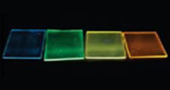
Semiconductor NPs, also called QDs, are different from bulk semiconductors in that optical properties of QDs depend on their size. In semiconductors that are several nanometers in diameter, an electron and a hole are confined in a smaller space than the exciton Bohr radius, so the quantum confinement effect is observed in all three dimensions. Because of this confinement, energy levels become discrete and the bandgap (BG) between valence band and conduction band is affected by the size of the NP. The BG is related to the process by which an electron is excited by light and stabilized. As QD size decreases, the BG increases, the wavelengths absorbed decrease, and fluorescence wavelength decreases
The BG is related to the process in which an electron is excited by light and stabilized. As QD size decreases BGs increases, shorter wavelengths absorbed decrease, and fluorescence wavelength decreases
(Fig. 1).
 Figure1. Effect of QD size on fluorescence wavelength after excitation by UV light.
QD core/shell structure can be classified into type-I and type-II (Fig. 2)
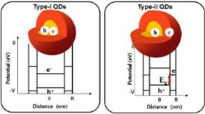 Figure2. Energy-level diagrams of type-Ⅰ and type-Ⅱ QDs
(e : electron, h : hole, Eg : BG).
Semiconductor QDs are categorized into two types. In type-I QDs, the energy BG is higher in the shell material than in the core material so the electron-hole pair is confined within the core; therefore type-I QDs are used to get high photoluminescence (PL) efficiency. In type-II QDs, the energy levels of the valence band and the conduction band of the core cross those of the shell, so some of the electrons are separated from their holes (Fig. 3a); because of this characteristic, type-II QDs can be used as energy-conversion materials in solar cells. Changes in the energy levels of the valence band and the conduction band of core and shell affect the charge density of electrons and holes in space. The change in energy levels also causes an ‘effective BG’ which is quite independent of the material that composes the QD, so the wavelength of absorption and the PL are controllable (Fig. 3).
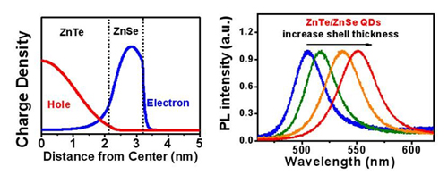 Figure 3. (Left) electron and hole residence probability densities; (right) PL spectra of ZnTe/ZnSe (core/shell) QDs (Chem. Mater. 2010, 22, 233-240).
Colloidal NPs that are synthesized from solution precursors can be tuned in morphology and size, so they have many potential applications. Control of the morphology of these NPs can affect their functionalities because it determines fine structures of internal energy states, carrier mobility in the particles, and the probability that an exciton exists at a given position. Morphology can be controlled by adjusting their nucleation and growth steps, which start from atom-level control. Those reactions are usually governed by both kinetics (reactant concentration, diffusion) and thermodynamics (quantity of surfactants, temperature). Solution-based synthesis methods yield highly-crystalline NPs with various shapes, and have noticeable advantages over typical top-down methods. We synthesize various types of NPs, including core/shell QDs, nanorods, nanotetrapods and nanoporous materials (Fig. 4a). Also, we have reported ‘supra QDs’ (SQDs) (Fig. 4b) which are superstructures composed of hundreds of QDs (each a few nanometers in size) assembled by oriented attachments; these SQDs may have high mobility as charge carriers; and therefore show great potential to sensitize solar cells.
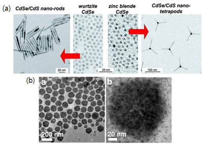 Figure 4. (a) TEM images of CdSe/CdS heterostructures (nanorods and nanotetrapods) by solution-based synthesis methods. (J. Phys. Condens. Matter, 2016, 28, 53001) (b) TEM images of CdSe supra-QDs
2. Investigation on the property of NPs induced from the incorporation of foreign atoms
Introducing a foreign atom into an as-synthesized NP causes changes in optical, electrical, and magnetic properties, in addition to composition change. Depending on the amount of impurity, it can be categorized in several ways. First, we can dope semiconductor NPs in the same way that bulk materials are doped.
Doping is the intentional introduction of foreign atoms into a pristine semiconductor host material for the purposes of modulating its optical, electrical, and magnetic properties. In bulk semiconductor material, dopants ionize to lend extra electrons or holes depending on the ion’s valence. The spin of a transition-metal dopant can couple with orbitals of the host material. Owing to those features, doped semiconductors are used in semiconductor junction structures such as transistors and diodes.
In contrast, doping in semiconductor NCs is affected by quantum confinement, so the process yields different behaviors than the bulk materials show. Confinement of excitons in an extremely small space increases its coupling with dopant ions, and as a result amplifies the modulation of their optoelectric and magnetic properties. Doped NCs have potentials to be used in various fields such as memory devices, photocatalysts and bioimaging probes, in addition to semiconductor junction structures.
Cation exchange is a method to introduce foreign atoms into a crystal lattice. Bonding between atoms in semiconductors is mostly ionic, so addition of new cation can eject original cations while preserving anions. Such transformations allow synthesis of sophisticated nanostructures such as metastable crystal structures or complex morphologies that are not easily accessible by using direct synthesis.
By controlling the quantity of foreign ions, cation exchange can be applied to doping or synthesis of heterostructures and completely new materials. The exchange reaction is driven by the relative difference in the thermodynamic stabilities of the reactant and product, by circumstantial ligand complexation. The feasibility of a reaction can be predicted by considering exchange conditions and the solubility product and standard enthalpy of formation of materials.
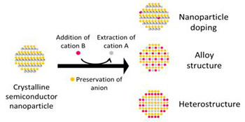 Figure 5. Cation exchange of NP
In NPs, although the constituent materials are the same, the crystal structures after cation exchange may be different from each other because the thermodynamic stability differs depending on the size (Fig. 6). Therefore, research into how the results of cation exchange depend on NP size is very helpful to understand the mechanism of the cation exchange reaction in NPs. After the cation exchange reaction, data from optical properties, X-ray diffraction pattern, energy-dispersive X-ray spectroscopy and other atomic analysis methods should be analyzed to confirm the composition and structure of the final material.
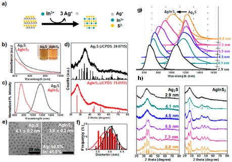 Figure 6. (a) Schematic representation of a cation exchange reaction of Ag2S NPs into AgInS2 NPs. cation exchange reaction of 4.1-nm NPs: absorption spectra (b), PL spectra (c), XRD patterns (d), TEM images (e), and size histogram (f) of samples before (Ag2S: black) and after (AgInS2: red) CE. PL spectra (g) and
XRD patterns (h) of a size series of Ag2S NPs before and after CE. (Chem. Mater., 2016, 28, 8123-8127)
Figure 6. (a) Schematic representation of a cation exchange reaction of Ag2S NPs into AgInS2 NPs. cation exchange reaction of 4.1-nm NPs: absorption spectra (b), PL spectra (c), XRD patterns (d), TEM images (e), and size histogram (f) of samples before (Ag2S: black) and after (AgInS2: red) CE. PL spectra (g) and
XRD patterns (h) of a size series of Ag2S NPs before and after CE. (Chem. Mater., 2016, 28, 8123-8127)
3. PL modulation of QD
The emission wavelength and intensity of QDs can be modulated, so they have possible application as switch probes for cellular and whole-body imaging, as optical modulators, and as light-emitting diodes. We used type-II QDs to develop a photoluminescence-modulating probe that reacts to external stimuli. Charging a type-II QD in which the electrons and holes are separated results in photoluminescence (PL) spectral switching. It returns to the initial state after a neutralization step. Reversible PL switching for many repeated cycles was demonstrated by alternating UV excitation between on and off (Fig. 7). Also, a modulating sensor based on PL on-off system was developed. Reversible and wavelength-selective PL modulation was also investigated by controlling the charge transfer between QDs and quenchers.
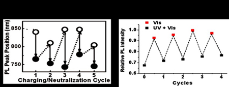 Figure 7. (left) Repeated PL spectral switching of type-II QD sample by multiple charging/neutralization processes. (right) QD PL switching by alternating on/off cycles of UV light under continuous visible light illumination.
(J. Phys. Chem. C, 2009, 113, 6320-6323)
Figure 7. (left) Repeated PL spectral switching of type-II QD sample by multiple charging/neutralization processes. (right) QD PL switching by alternating on/off cycles of UV light under continuous visible light illumination.
(J. Phys. Chem. C, 2009, 113, 6320-6323)
4. QD-based Solar Cells
A solar cell (SC) converts light energy directly to electrical energy. Silicon SCs have been deployed on a commercial scale but they are expensive and require a complicated fabrication process. SCs can be fabricated easily and inexpensively using NPs. Several kinds of SC use QDs, including QD-sensitized SCs, Hybrid-type SCs (QD/conducting polymer; Fig. 8) and Schottky-type SCs.
These SCs have different structures, but all of them generate and transfer charge by absorbing light. Charge separation and transfer are affected by the shapes of the QDs and the form of the active layer. By using QDs for SCs, the wavelength absorbed can be controlled; furthermore, QDs can be easily dispersed using various solvents, so development of SCs that use QDs is a promising avenue of research. Experiments can determine conditions under which SCs based on QDs can reach high power conversion efficiency, and the insights gained may guide development of simple methods to fabricate QD SCs at low cost.
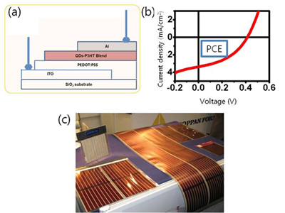 Figure 8. (a) Structure of the hybrid type SCs, (b) I-V curve of a hybrid type SC, (c) Image of a commercialized next generation SC (ref.: http://www.konarka.com).